Silicon, Silicon Carbide & Piezo Ceramics
Applications
General
- Active Devices NOT Mechanically or Electrically Damaged by processing
- Any shape required–shape complexity is not a limitation
- No hard tooling or non-recurring engineering charge
- No tooling impact for design changes
- Fast delivery of any custom shape or size
- Economical small lot quantities
Types
- Optoelectronic Detectors
- Die Placement Templates
- Shadow Masks
Uses
- Down Sizing of Silicon Wafers
- Excising non-rectangular devices
- Reactive Ion Etcher Gas Metering Electrodes
Materials
- Silicon Wafers
- Any Dopant or Crystal Orientation
- Silicon Carbide
- Piezo Ceramics

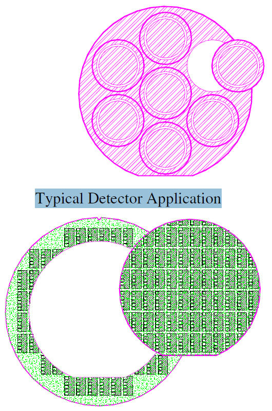
Typical Down sizing Application
