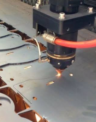
Silicon Machining
Questech Services Corporation offers YAG LASER silicon machining for a variety of applications. Silicon downsizing or coring is one of the more interesting applications of YAG LASER silicon machining. This is most noteworthy and commonly used in three ways:
First of all, reduction in size of a blank silicon wafer such as a 200 mm wafer to a 150 mm wafer for special requirements of processing in a 150 mm wafer fab.
In addition, reduction in size of a completed “live” 200 mm silicon wafer to a 150 mm wafer for accommodation in a limited size tester or other “backend” machine.
Finally, excising numerous completed “live” smaller non-rectangular parts from an array on a large “live” silicon wafer.
Additional Special Processes
Especially relevant, there are several important additional processes that Questech can provide:
First, before processing, application by a semiconductor photo resist spinner of positive photo resist to protect the fragile “live” wafer surface from detritus ejected during the LASER cutting process. Afterward, the positive resist is easily stripped with acetone, among other chemicals, and should be left on the wafers for shipment back to the customer.
Inclusion of a specified dimension wafer edge flat critically aligned to an existing wafer flat. This is accomplished by careful optical edge alignment in the YAG LASER machining system at high magnification.
In addition, application of “Semi standard” font or other special font LASER marking and serialization to the machined parts.
Next, processing through a silicon wafer edge grinder to produce the required radiused edge for compatibility with wafer handling techniques. This will be done to specified typical semiconductor industry standards.
Finally, special packaging of machined silicon parts as specified.
In conclusion, decades of silicon machining experience ensure that Questech pays attention to the critical factors. Specifically, alignment accuracy, ESD protection, safe handling, storage and cleanliness of valuable silicon material.